Diagnostics Update: VTref = 3.238V [CONFIRMED POWER OK]
Your latest run successfully verified that the J-Link senses target power (VTref=3.238V). The SWD connect failure (Could not connect to target device) is caused by bus contention or clock speed. Follow the diagrams below to verify Jumper CN1, Pogo Pin Seating, and run the optimized flasher.
SEGGER J-Link EDU Mini — 10-Pin Cortex-M Header & Ribbon Cable
Standard 1.27mm (0.050") 2×5 Pin Header (Samtec FTSH-105-01-L-DV Compatible)
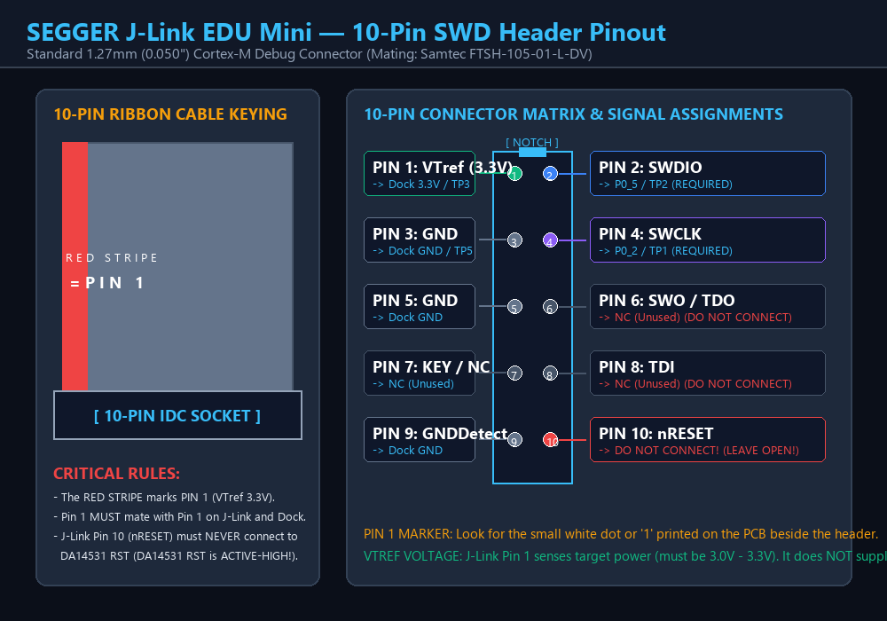
| Pin # | Signal Name | Ribbon Stripe | Electrical Direction | Dock Header (CN2) | Capsule / DA14531 Destination | Hookup Rule |
|---|---|---|---|---|---|---|
| Pin 1 | VTref (3.3V) | RED STRIPE | Input to J-Link (Senses Target) | CN2 Pin 1 (V3.3) | TP3 (VDD_3V3 System Rail) | MANDATORY (Must measure ~3.24V) |
| Pin 2 | SWDIO / TMS | Pin 2 adjacent | Bi-directional SWD Data | CN2 Pin 2 (POGO_TX) | DA14531 Pin P0_5 / TP2 | MANDATORY (Serial Wire Data) |
| Pin 3 | GND | Red stripe side | Power Ground Return | CN2 Pin 3 (GND) | Dock GND / TP5 | MANDATORY (Ground Reference) |
| Pin 4 | SWCLK / TCK | Second column | Clock Out from J-Link | CN2 Pin 4 (POGO_RX) | DA14531 Pin P0_2 / TP1 | MANDATORY (Serial Wire Clock) |
| Pin 5 | GND | Red stripe side | Ground Return | CN2 Pin 5 (GND) | Dock GND | Tied internally to GND |
| Pin 6 | SWO / TDO | -- | Serial Wire Output (Trace) | NC (Unconnected) | Not supported on DA14531 | LEAVE UNCONNECTED |
| Pin 7 | KEY / NC | -- | Keying Pin / Unused | NC (Unconnected) | -- | LEAVE UNCONNECTED |
| Pin 8 | TDI | -- | JTAG Data In | NC (Unconnected) | Not used in SWD mode | LEAVE UNCONNECTED |
| Pin 9 | GNDDetect | Red stripe side | Ground Sense | CN2 Pin 9 (GND) | Dock GND | Tied internally to GND |
| Pin 10 | nRESET | Second column | Active-Low Reset Output | NC (Unconnected) | DO NOT HOOK TO DA14531! | CRITICAL WARNING: DA14531 RST IS ACTIVE-HIGH! |
How to orient the Ribbon Cable:
The 10-pin ribbon cable supplied with your J-Link EDU Mini has one wire marked with a solid RED STRIPE. This red wire is Pin 1. Always ensure the red stripe aligns with the white dot or "1" printed beside the CN2 box header on the dock PCBA.
Charging Dock PCBA (NN-DOCK-01) — Component & Header Map
Component locations, Jumper CN1 requirement, and CN2 J-Link header routing
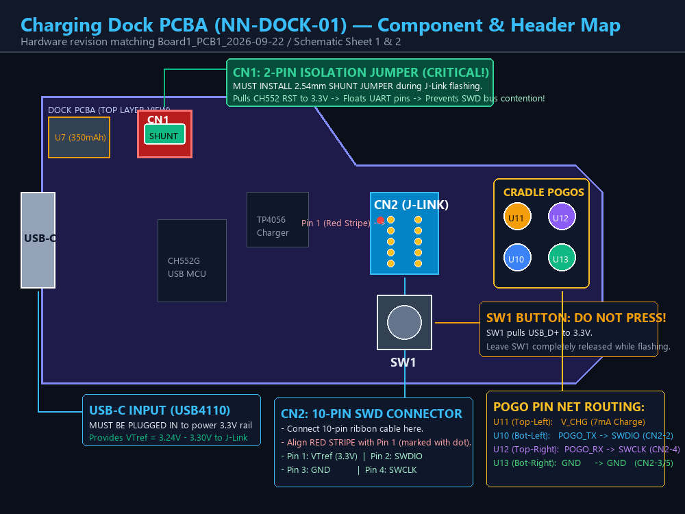
CN1: 2-Pin Bus Isolation Jumper (MUST BE INSTALLED)
The dock PCBA contains an onboard CH552G USB microcontroller that normally controls the pogo pins for UART communication. Pin 1 of CN1 is tied to 3.3V, and Pin 2 connects directly to CH552 Pin 6 (RST).
CN2: 10-Pin J-Link Box Header
The shrouded box header (hanxia HX JN1.27-2x5) receives the J-Link 10-pin ribbon cable. Pin 1 is marked with a white dot or notch.
- Pin 1: V3.3 Target Voltage Reference (VTref)
- Pin 2: POGO_TX -> SWDIO (P0_5)
- Pin 3/5/9: GND (System Ground)
- Pin 4: POGO_RX -> SWCLK (P0_2)
USB-C Power Delivery Input (USB1)
J-Link EDU Mini does not supply power to the target board. The USB-C port must be connected to a USB port or charger to energize the dock's 3.3V voltage regulator. This is what provides VTref = 3.24V to the J-Link.
SW1 Push Button (DO NOT PRESS)
The tactile switch SW1 is connected between 3.3V (via a 10k resistor) and USB D+. It is used for dock firmware updates or wake events. During J-Link flashing, leave SW1 completely released. If pressed, it can pull USB lines into abnormal states.
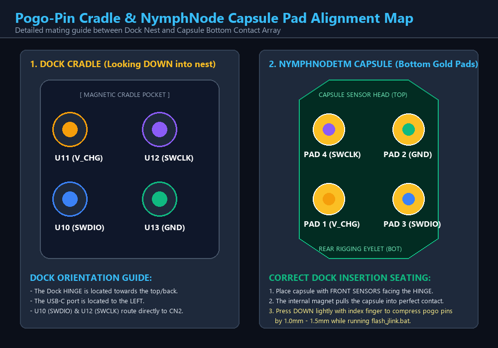
Pogo-Pin Cradle & NymphNode Capsule Pad Alignment Map
Exact mating correlation between dock spring pins and the capsule's 4 gold pads
| Dock Pogo Pin | Dock Physical Position | Capsule Mating Pad | Capsule Bottom Location | DA14531 / Circuit Net | J-Link SWD Route |
|---|---|---|---|---|---|
| U11 | Top-Left of cradle nest | PAD 1 | Lower-Left (near rear eyelet) | V_CHG (7mA LiPo Charging Input) | -- (Powered via Dock LDO) |
| U10 | Bottom-Left of cradle nest | PAD 3 | Lower-Right (near rear eyelet) | P0_5 / POGO_SWDIO_UART | CN2 Pin 2 (SWDIO) |
| U12 | Top-Right of cradle nest | PAD 4 | Upper-Left (towards sensors) | P0_2 / I2C_SCL / SWCLK | CN2 Pin 4 (SWCLK) |
| U13 | Bottom-Right of cradle nest | PAD 2 | Upper-Right (towards sensors) | GND (Common Ground Return) | CN2 Pin 3/5/9 (GND) |
Seat the capsule with its tapered front sensor tip pointing toward the dock hinge. The rear rigging eyelet should face outward toward you.
The internal N52 neodymium magnet will snap the capsule into its indexed seat. If the capsule resists or wobbles, check for reverse 180° rotation.
While executing flash_jlink.bat, press down gently on the center of the capsule with your index finger to compress the pogo plungers by 1.0mm.
NymphNode Direct PCBA Test Pads (Pre-Potting Flying Wires)
For direct bench debugging using micro-hook probes or fine 32-36 AWG solder wires
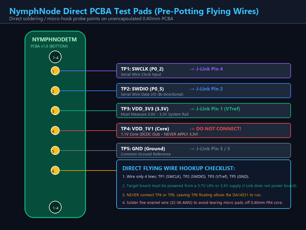
TP4 is the regulated output of the DA14531's internal step-down buck converter (1.10V core rail). Connecting 3.3V or J-Link Pin 1 to TP4 will immediately burn out the silicon core. Leave TP4 untouched.
Unlike standard ARM Cortex chips that use active-low reset (nRESET), the Dialog/Renesas DA14531 uses an ACTIVE-HIGH reset. Pulling TP6 HIGH forces the CPU into reset, disabling SWD communications. Leave TP6 open.
Capsule Core Power & BQ29700 Wake-Up (In vs Out of Cradle)
Verifying battery voltage, protection IC sleep latch, and cradle mating alignment
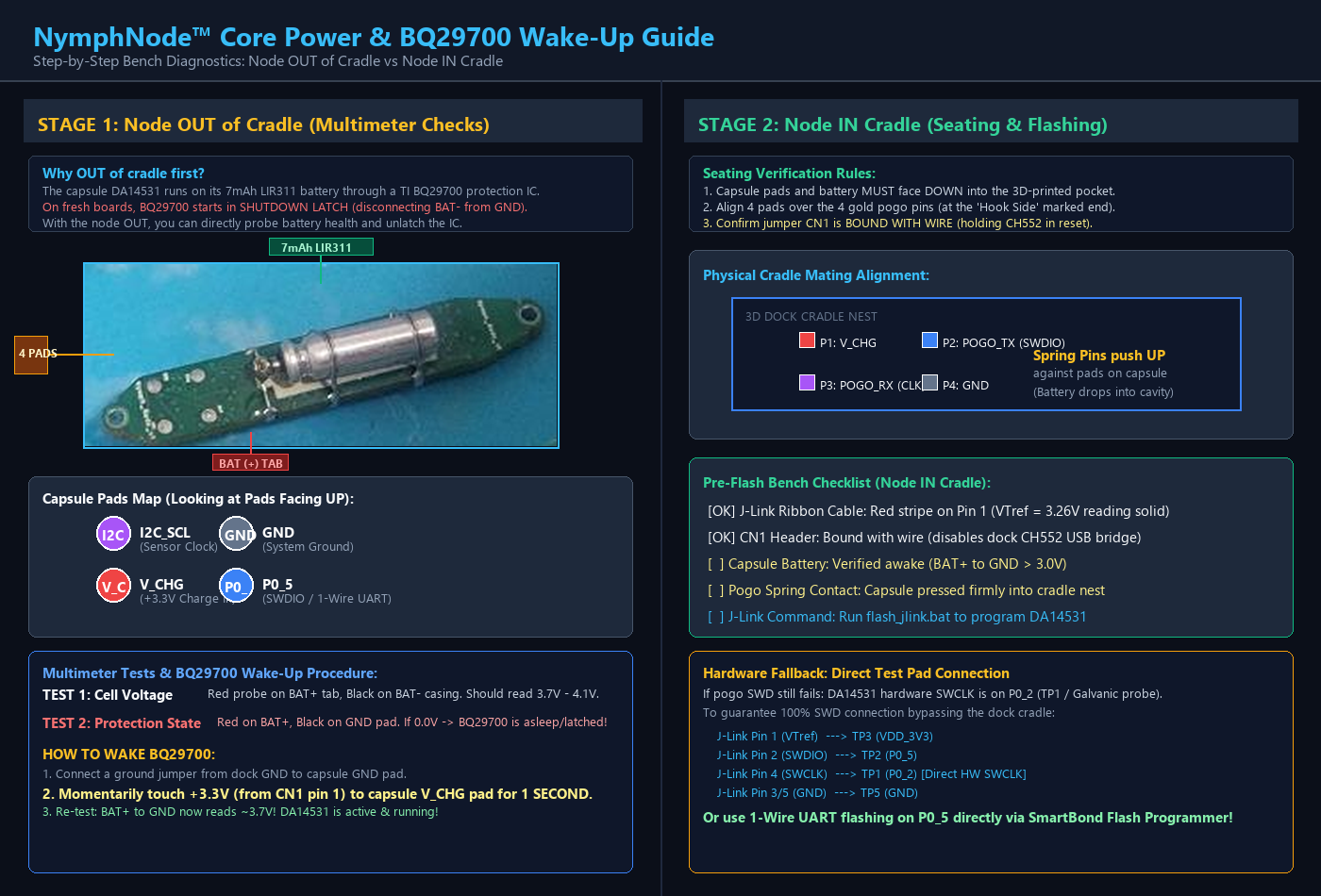
The Renesas DA14531 runs exclusively on the internal 7mAh LIR311 secondary lithium battery via a Texas Instruments BQ29700 battery protection IC. On new or disconnected capsules, the BQ29700 stays in shutdown sleep mode, disconnecting BAT- from system ground.
Touch Red multimeter probe to BAT(+) tab (solder joint next to pads) and Black probe to BAT(-) casing.
If this reads 0.0V, the BQ29700 is asleep! The DA14531 has zero power.
Connect a wire from dock GND to capsule GND pad. Momentarily touch +3.3V (from CN1 Pin 1) to capsule V_CHG pad for 1 second. Re-test: BAT+ to GND now reads ~3.7V, and the core is active!
Once the capsule battery is confirmed awake, seat the capsule into the 3D-printed dock cradle to establish pogo contact:
- The 4 gold pads and the battery cylinder MUST face DOWN into the cradle cavity.
- The end with the 4 pads (labeled
Nymph_Node_v1) sits over the 4 gold pogo pins (marked "Hook Side"). - Press lightly on the capsule to ensure the 4 spring pogo pins compress.
- CN1 Jumper: Bound with wire (confirmed! CH552 held in reset).
- J-Link VTref: Reads 3.26V solid from dock rail.
- Run
flash_jlink.batinFirmware/tools/.
Breadboard Wire Mapping: Charging Dock (Red) ➔ NymphNode (Blue)
Exact 1-to-1 jumper wire guide resolving all 180° rotation and mirroring ambiguities
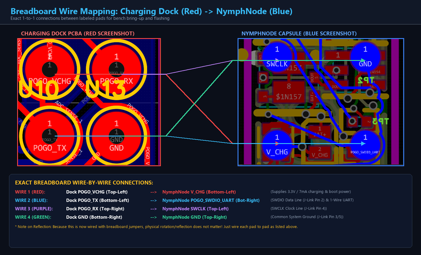
| Jumper Wire | Dock Pad (RED Screenshot) | Direction | NymphNode Pad (BLUE Screenshot) | Electrical Function |
|---|---|---|---|---|
| WIRE 1 (RED) | POGO_VCHG (Top-Left) | ➔ | V_CHG (Bottom-Left) | Supplies 3.3V charging & system boot power |
| WIRE 2 (BLUE) | POGO_TX (Bottom-Left) | ➔ | POGO_SWDIO_UART (Bottom-Right) | SWDIO Data Line (J-Link Pin 2) & 1-Wire UART |
| WIRE 3 (PURPLE) | POGO_RX (Top-Right) | ➔ | SWCLK (Top-Left) | SWCLK Clock Line (J-Link Pin 4) |
| WIRE 4 (GREEN) | GND (Bottom-Right) | ➔ | GND (Top-Right) | Common System Ground (J-Link Pin 3/5) |
In the 3D-printed dock cradle, the NymphNode was placed face-down, meaning the top-to-bottom and left-to-right rows crossed over mechanically. Now that you are using individual wires on a breadboard, mechanical rotation and reflection do not matter at all! Simply route each jumper wire directly from the dock pad to the NymphNode pad according to the table above.
4-Step Checklist to Connect & Flash Right Now
Resolve the "Could not connect to target device" error and complete firmware bring-up
Install CN1 Jumper
Locate the 2-pin header labeled CN1 above USB-C on the dock PCBA. Place a standard 2.54mm plastic shunt jumper across both pins.
Align Ribbon Red Stripe
Ensure the RED STRIPE on the 10-pin ribbon cable aligns with Pin 1 (marked with a white dot) on header CN2.
Firm Cradle Seating
Place the NymphNode capsule into the magnetic nest with sensors toward the hinge. Press down lightly with your index finger to compress the pogo springs by 1mm.
Run flash_jlink.bat
Double-click flash_jlink.bat in Firmware/tools/. The SWD clock speed is now set to a stable 400 kHz.